ASICs: Custom Chips to Improve Performance
The benefits of ASICs. How custom silicon can make a company's "beer taste better". AI accelerators. The rationale behind Broadcom and Marvell's ASIC design service.
This article discusses custom silicon chips and why companies like Google, Amazon, Meta, and Microsoft are choosing these over standard CPUs and GPUs. If you’re new to the topic, watch this short video that showcases Amazon's custom silicon and rationale.
▶️ Video: Inside the Making of an AI Chip
Single Purpose Chips
In previous articles we’ve studied general-purpose logic chips that help systems think including the CPU and GPU. We now shift our focus to the other end of the spectrum— purpose built chips called Application Specific Integrated Circuits (ASICs)1.
📖 ASIC: a custom chip for a specific task
Purpose built ASICs put the hard in hardware. The chip is the algorithm. It’s a specific circuit built for a single job. We’ll walk through several illustrative examples later in this article.
Why Custom Silicon?
Writing software for general-purpose processors is getting easier and cheaper by the day — thanks GitHub Copilot! Access to compute is also easier and cheaper too — thanks cloud computing! As a result, finding product-market fit for a software-based business idea has never been easier.
📖 product market fit: when a product successfully meets the needs and wants of its target customers
Why then, would a company opt for custom silicon?
It turns out that general-purpose processors are less efficient at any given task by design. These processors support a broad range of instructions at the cost of increased latency, power, and chip size. This overhead is okay when doing many different tasks, but not needed when repeating the same task.
For example, why take time to fetch and decode the same instructions again and again if you’re only doing a single job? A custom chip is a circuit hardcoded to do the algorithm - it doesn’t need instructions.
Conceptually, ASICs cut away all unnecessary execution and unused circuitry of a general-purpose chip. Designing a chip without overhead means ASICs have reduced latency, power consumption, and/or chip size compared to general-purpose processors.
💡For a given task, ASICs offer better performance with lower energy use than general-purpose processors
Companies that are running a particular task repeatedly on general-purpose hardware have the opportunity to improve performance and reduce power with a custom ASIC, especially at scale.
💡 ASICs are advantageous when the same task is frequently executed on general-purpose hardware and there is a need to minimize overhead
Benefits
Switching to custom silicon has many benefits.
Large cloud service providers can accumulate significant performance per watt improvements from custom chips. The gains can be “spent” improving the customer experience, reducing operational costs, or both. In consumer markets, ASICs can improve a product’s user experience, for example increasing the battery life of wearables. ASICs help embedded products combine several discrete parts into a single chip, making the system simpler, streamlining supply and manufacturing, and increasing reliability.
Later in this article, we will look at real-world examples that showcase these benefits.
ASIC Flexibility
You might wonder if the single-purpose nature of ASICs constraining. What if the solution requires a bit of flexibility?
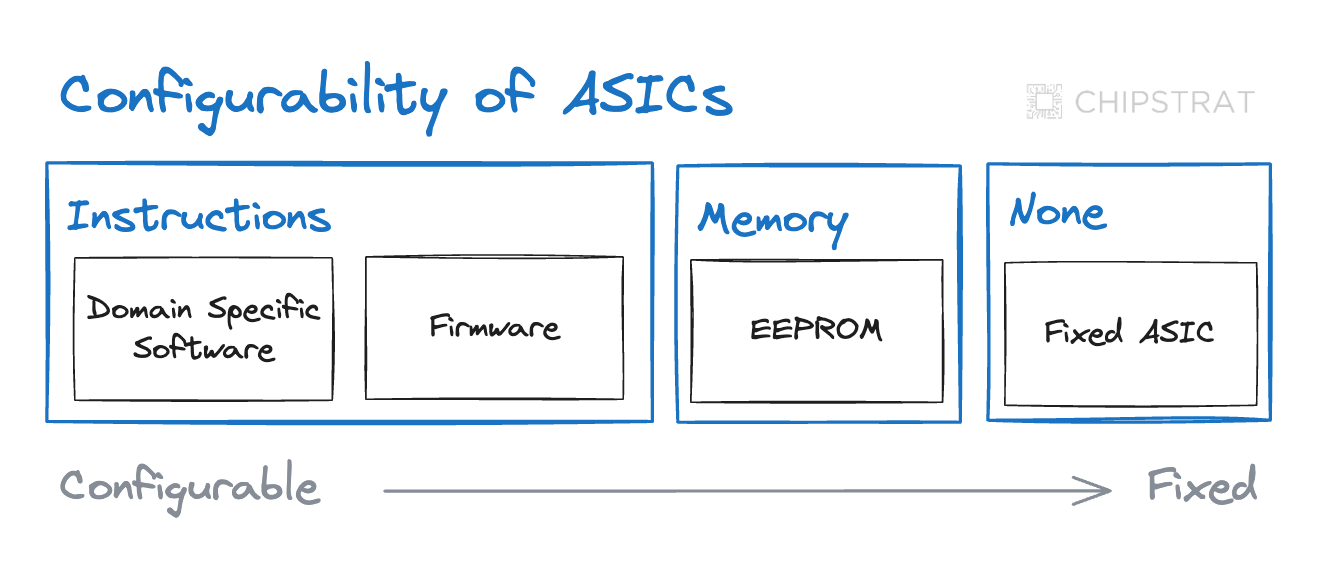
ASICs offer varied flexibility levels. Some can run limited software, others can only read data from memory, and some are non-configurable.
The inflexible end of the spectrum is a good place to conceptually anchor when you think about ASICs. Remember - the chip is the algorithm.
When slight adaptability is required, such as for storing device configurations, ASICs can be modified using data. For example, a chip that reads default settings from a device's memory and allows system designers to update the values in memory post-manufacturing. A common approach uses Electrically Erasable Programmable Read-Only Memory (EEPROM) to store configuration data and retain it when power is removed.
📖 EEPROM: a type of memory that retains data without power and can be electrically erased and reprogrammed
Consider a kitchen light as an analogy. It's a basic circuit — turn on the switch and the bulb emits light at 100% brightness. This resembles an ASIC with no adjustability. For some, this default output is too bright, so a dimmer switch can be added to the circuit to allow the user to tune the brightness to their liking. The dimmer switch circuit is like an ASIC with simple configurability.
Various ASICs have special software called firmware built into them when they're made. This firmware is the specific set of instructions that makes the ASIC do its particular job and is integrated into the chip during manufacturing. Firmware gives ASICs a degree of flexibility, as chip manufacturers can send updates to customers for reasons like fixing bugs, patching security vulnerabilities, or enhancing performance.
📖 firmware: Infrequently updated instructions that govern a chip's functionality
Finally, some ASICs like domain-specific hardware accelerators2 allow users to efficiently run software for a particular domain such as machine learning or audio processing.
📖 domain-specific hardware accelerator: an ASIC optimized to run domain-specific tasks faster and more efficiently than standard processors
AI accelerators are an example of a domain-specific accelerator built for efficient parallel processing of matrix multiplications, a key mathematical operation in machine learning. Their architecture is designed to accelerate AI software, hence the name AI accelerator.
📖 AI accelerator: an ASIC specifically designed for the efficient processing of AI workloads
AI accelerators are configurable in the sense that they will efficiently run any computational workload involving matrix multiplication; they aren’t limited to only a single algorithm.
The Google TPU (Tensor Processing Unit) is an example of an AI accelerator and can accelerate a variety of ML-enabled workloads such as recommendation systems, fraud detection, chatbots, and more.
Purpose-built processors can feel conceptually murky – they have similarities to both general purpose processors and fixed ASICs. Where should they belong in our mental model? It’s easiest to think of these hardware accelerators as the middle ground between general-purpose processors and fixed ASICs.
Spend Money to Make Money
Developing a custom chip involves significant financial investment, especially upfront non-recurring engineering (NRE) costs. Check out Sigenics’ highly explanatory walkthrough of the ASIC design process to learn more and see ballpark costs of each step.
📖 Non-recurring engineering costs: one-time expenses incurred designing and developing an ASIC, including design, testing, and preparing for chip production.
Investing in an ASIC can offer varied returns and savings such as reduced energy and infrastructure costs, improved efficiency, increased market share, or lower cost of goods sold. The math can easily work for tech giants, but as Sigenics points out, it can also pencil out for small and midsize customers depending on the use case.
Take note of the opportunity cost of custom silicon, which requires significant investment in time, finances, and personnel, potentially diverting resources from alternative projects. The investment in custom silicon must pay dividends for a beyond just cost savings; ideally, the performance and power savings can be “spent” to create a differentiating advantage.
As Jeff Bezos emphasizes, “Focus on the things that make your beer taste better”.
We’ll see this in the examples below.
📖 Opportunity cost: the potential profit lost from a missed opportunity
💡Use ASICs when they make your company’s beer taste better AND the costs pencil out
Lessons From Real-World ASIC Examples
Bitcoin mining and YouTube video transcoding are prime examples of ASICs outperforming general-purpose processors.
Bitcoin mining
We’ll examine the progression of hardware in Bitcoin mining to showcase the advantages of ASICs.
As a quick reminder - Bitcoin is a cryptocurrency, and Bitcoin mining is the process by which new Bitcoins are created. If you’re not familiar with Bitcoin or how it’s mined, here’s an analogy:
Bitcoin is like a global lottery where everyone can use a computer to generate lottery tickets. The first to find the winning ticket wins some Bitcoin. The game gets harder over time to make sure someone wins only once every 10 minutes on average.
Participants typically begin the race with a personal computer, but soon realize that a single laptop's odds of winning are low. To improve their chances, they might add more computers for higher throughput, invest in faster computers to reduce latency, or do both.
CPU to GPU to ASIC
In the early stages of Bitcoin mining, miners used CPUs to run mining algorithms. Competition was limited and the network difficulty was low, so the “odds of winning” were higher.
Participants realized that mining's repetitive, parallel tasks are ideal for a GPU and it’s thousands of cores which can mine Bitcoin in parallel3. GPU-based mining improved throughput by 10-100x, significantly increasing the likelihood of successful Bitcoin mining. The total cost of ownership (TCO) of GPUs remained comparable to that of CPUs, resulting in a significantly improved ROI for GPU mining. As a result, miners universally transitioned to GPUs for mining.
📖 Total cost of ownership: costs associated with buying, operating, maintaining, and eventually disposing of hardware.
Here’s where ASICs come in! Observing that Bitcoin mining repetitively uses the same algorithm on general-purpose hardware, forward-thinking companies developed Bitcoin ASICs. These ASICs have no unnecessary general-purpose GPU overhead and they don’t waste chip area — it’s all mining, all the time. They have even better performance per watt than GPUs, increasing the odds of successful mining while also consuming less electricity.
ASIC miners aren’t cheap, but they have several orders of magnitude performance improvements at roughly the same order of magnitude in TCO as a GPU. This led to the rise of Bitcoin farms that house hundreds of thousands of ASIC miners4
The vast majority of profitable Bitcoin mining is now conducted using ASICs.
Logarithmic benefits of Bitcoin ASICs
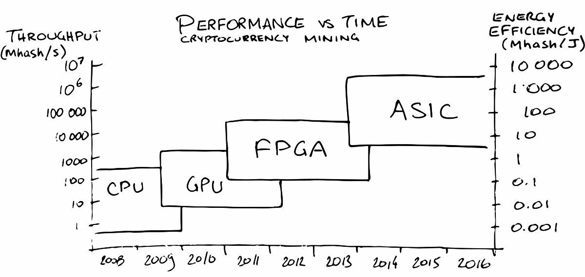
This awesome chart5 illustrates the progression in throughput as mining shifted from sequential CPUs to parallel-processing generic GPUs and eventually to custom ASICs. Note that the Y axis is logarithmic, so the throughput and energy efficiency of an ASIC can be more than 10,000x a CPU!
Reconfigurable hardware, such as FPGAs, occupies a middle ground between general-purpose hardware (CPUs & GPUs) and custom-designed integrated circuits (ASICs). We'll dive into reconfigurable hardware in a future discussion.
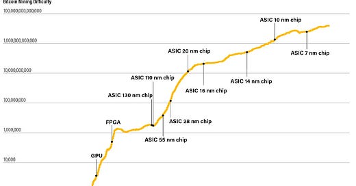
Below is a useful chart6 illustrating the increasing mining difficulty as a function of increasingly smaller fabrication process nodes of ASICs. The increasing network difficulty was driven by an increase in network performance from more potent ASICs.
📖 process node: the technology used to make chips as measured by the smallest transistor feature size. Smaller nodes lead to more advanced, efficient, and powerful chips.
The key takeaway from the evolution of Bitcoin mining hardware is the supremacy of ASICs over general-purpose GPUs in terms of performance, leading to the dominance of ASIC chip manufacturers in the market.
💡 ASICs are capable of rapidly taking market share from solutions that rely on general-purpose processors
Google Video Transcoding
The Argos VCU, developed by YouTube, is a great example of investing in custom silicon to “make your beer taste better”.7
Google data centers use significant compute resources processing YouTube videos, specifically transcoding videos into various formats8 to ensure compatibility across a range of devices and internet speeds. Traditional CPUs are not the most efficient for this task. Considering that roughly 500 hours of video content are uploaded to YouTube every minute, any improvements to transcoding on such a massive scale really add up.
As explained by YouTube vice president Scott Silver to Protocol,
“If most of your computers are transcoding videos and you’re paying many tens of millions or hundreds of millions of dollars a year to do that, it would become obvious that you have room to [invest in] an ASIC to do that.”
Google developed an ASIC for video transcoding called a Video transCoding Unit (VCU). Coupled with new custom software, this system is designed for large-scale, reliable transcoding. The VCU-powered system shows a 20x-33x improvement over previous CPU and GPU based systems.
These cost savings can be compelling for C-suite decision-makers. Yet YouTube also emphasized their investment in custom silicon was to “make their beer taste better” and used the performance savings to create a better user experience for customers.
“Our focus is not really on saving money,” Silver said. “We like saving money, but what we really want to do is deliver an as-good — if not a better — quality experience for viewers.”
“The thing that we really want to be able to do is take all of the videos that get uploaded to YouTube and transcode them into every format possible and get the best possible experience.”
The transition to custom ASIC with Argos VCUs not only improved YouTube’s user experience but also lowered infrastructure expenses. Dylan Patel estimated that YouTube's shift from Intel CPU servers to Argos VCUs for video transcoding reduced its Intel server CPU purchases by approximately 10 million units!
YouTube’s VCU is a case study in the massive impact an ASIC can have for hyperscalers and their customers.
💡Using a general-purpose chip when running the same algorithm repeatedly can be inefficient, so it's worth checking if a specialized ASIC could do the job better.
The rest of this article, accessible to paid subscribers, will discuss why merchant silicon companies like Marvell and Broadcom are doing custom silicon. We’ll also review the tech giants making their own custom silicon including AWS, Meta, Microsoft, and Google.


