It’s time for another educational post. We’ve covered logic chips and memory, but for a change of scenery, let's explore semiconductor manufacturing.
Today’s topic is metrology – the science of measurement.
Don’t be scared by the name “metrology”; it sounds dense and boring, but not so! We’ll broadly discuss metrology in manufacturing and then venture into semiconductor metrology.
Metrology in Manufacturing
What kind of measurements are useful in manufacturing?
Physical dimensions like length, width, and diameter come to mind. It’s easy to imagine why dimensions matter during manufacturing; a two-by-four wood plank should be exactly 2 inches by 4 inches, right? (Wrong! 😂)
Material properties like hardness and conductivity can also be measured. How well does this fiber optic line conduct light? How rigid is this door panel?
Surface measurements are also important. An iPhone's touchscreen glass is not only very hard but also very smooth; these characteristics are closely measured during manufacturing.
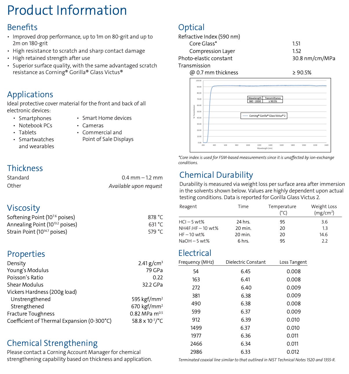
Corning’s Gorilla Glass (Victus® 2) product sheet illustrates a variety of mechanical, optical, chemical, and electrical measurements that are important for consumer device manufacturers:
Purpose of Metrology
Why is metrology important in manufacturing?
As demonstrated by the Corning Glass example, certain products are characterized by these measurements, which represent the product’s specs.
Metrology also provides the manufacturer with insights into quality assurance for finished products. How many final products met our desired spec?
Taking measurements during manufacturing catches defects early, saving resources by stopping work on flawed products.
Metrology can also offer a glimpse into future performance and reliability. For example, by analyzing measurements captured during production, Goodyear could predict whether a rubber tire might fail prematurely.
Metrology can also ensure regulatory compliance. Consider pharmaceuticals: Is the correct amount of active ingredient in this drug?
Metrology is the backbone of modern manufacturing, even more so in semiconductor production where precision at the atomic scale is essential.
Semiconductor Metrology
Making a modern chip can involve thousands of steps:
And each step can introduce quality problems!
It’s almost unbelievable that a 3-month process with thousands of steps yields chips that work. What’s even crazier is that these transistors are on the order of hundreds of atoms, and at this nanoscale, manufacturing is fundamentally probabilistic.
Inherently Probabilistic Manufacturing
Semiconductor manufacturing is inherently probabilistic, meaning the same process will naturally produce various outcomes. One wafer might end up with a thicker layer of material than planned, while another might have a thinner layer.
You might wonder why these processes aren’t deterministic, given that the manufacturing tools follow the same instructions repeatedly. The answer lies in the inherent randomness at the atomic level. These tiny differences ultimately lead to a range of outcomes in the final product:
Take copper interconnects as an illustrative example.
Copper is a popular choice for interconnects in modern semiconductors, and at first glance, it seems like the ideal material for wiring transistors together given its low electrical resistivity and high thermal conductivity. However, a closer look at copper interconnects at the atomic level reveals a polycrystalline structure, which means the copper is composed of numerous small crystals or "grains". These grains have random crystallographic orientations:


The boundaries between these grains cause electron scattering, which reduces electron mobility and negatively impacts electrical and thermal conductivity. Simply put, electricity and heat can’t travel as well in materials with random polycrystalline structure.
To make matters worse, as the dimensions of copper interconnects shrink, the impact of scattering from grain boundaries and surface boundaries becomes increasingly problematic:
The point of this digression is to highlight how inherent material randomness negatively impacts semiconductor chips.
Interconnects are just one example—copper interconnects, in fact, are some of the largest features on a chip.
At even smaller scales, like in transistors, inherent randomness causes variability in several ways. Dopant randomness occurs because transistors contain only a limited number of dopant atoms, leading to inconsistent dopant placement and uneven electrical properties. Channel and gate thickness variations result from slight imperfections during deposition or etching, altering electrical behavior like threshold voltage. Line edge roughness from photolithography and etching creates jagged boundaries that scatter electrons, increasing resistance and reducing performance.
Oh, and I haven’t even mentioned the quantum effects that cause problems at such small dimensions!
For example, gate leakage occurs when electrons “tunnel” through energy barriers that classical physics would deem impassable, allowing a small current to flow even when the transistor is off. Quantum tunneling can also cause transistors to switch at different voltages, resulting in timing mismatches and circuit errors.
Now, recall that a modern CPU or GPU has billions of transistors—and each transistor is slightly different! 🤯 wut? how do chips even work?
Chip designers use methods to mitigate poor-performing transistors and circuits, such as turning off sections of the chip that fail to meet standards and running the chip at lower clock speeds to reduce timing errors. Binning is also a common strategy; high-performing chips are sold as premium processors and those with defects that run slower are marketed as lower-tier products.
Of course, these are just workarounds. Wouldn’t it be best to find those issues as soon as possible during production instead of working on a chip for months and then discovering that it’s defective at the end of the process?
Metrology During Manufacturing
Instead of waiting until the end of production, inline metrology tools monitor the production process in real-time, allowing manufacturers to catch and fix problems as they arise. This metrology data is fed into statistical process control systems that detect deviations and enable on-the-fly adjustments like tool recalibration or parameter tuning. Engineers can track metrology data over time to further dial in the manufacturing process.
Metrology tools are vital not only during high-volume production but also from the initial stages of R&D and process technology development to test chip fabrication and low-volume production. For example, during process qualification, metrology ensures processes stay within tight tolerances, and as manufacturing scales, metrology helps engineers maintain consistent quality.
Trade-offs
Of course, everything comes with trade-offs, even the simple act of taking measurements during semiconductor manufacturing.
Metrology tools take up space in the fab and add time to wafer processing. Many metrology techniques require dedicated test wafers or use portions of product wafers for measurements. Last but not least, metrology tools are expensive to purchase and maintain.
Yet, these trade-offs are worth it. As imec says: “If you can’t see it, you can’t develop and control it.”
Looking Ahead
Metrology isn’t a solved science. Due to transistors’ ever-shrinking size and the need for non-destructive measurements, not every aspect of semiconductor manufacturing can be accurately characterized today.
Some inline metrology tools lack the resolution to detect atomic-level defects, such as dopant fluctuations or crystal imperfections. Measuring 3D structures, like FinFETs or GAA transistors, is challenging because many tools struggle to accurately capture vertical features and sidewall profiles. Certain process-induced defects require slow, specialized tools unsuitable for high-throughput production. Finally, subtle electrical issues, such as electromigration or bias temperature instability, often cannot be measured in real-time and are only detectable through post-manufacturing testing.
These are all challenges the industry is trying to solve. Startups included! Wait, you’re telling me there are semiconductor startups that aren’t building a proprietary AI accelerator? 😎
To learn more about some of the metrology big dawgs, here are links to their offerings:
If you know of interesting metrology startups, send them my way!


